Table of Contents >> Show >> Hide
- Why “Another KiCad Tutorial” Is Actually News
- The Tutorial That Sparked the “Wait, This Is Actually Learnable” Moment
- The Modern KiCad Workflow (The Part Tutorials Should Tattoo on Your Forearm)
- What’s Newer on the Scene: Tutorials That Match Where KiCad Is Now
- The Secret Weapon Most Tutorials Ignore: Add-ons, Plugins, and Quality-of-Life Tools
- How to Choose the Right “New KiCad Tutorial” for You
- Common Beginner Mistakes (and How Good Tutorials Prevent Them)
- Wrap-Up: A Tutorial That Teaches a Workflow Is a Gift to the Community
- Extra: of Real-World KiCad Experience (So You Don’t Have to Learn the Hard Way)
- SEO Tags
KiCad has always had that “free as in beer, powerful as in ‘why is this dialog box judging me?’” reputation. It’s a professional-grade, open-source EDA suite that can take you from schematic capture to a finished PCByet beginners often bounce off the first time they try to place a symbol, link a footprint, and realize they’ve accidentally created a library situation worthy of a true-crime podcast.
That’s why a genuinely well-scaffolded KiCad tutorial feels like a small miracle: it doesn’t just teach buttonsit teaches a workflow. And when a new tutorial arrives that respects your time (and your sanity), the community notices.
Why “Another KiCad Tutorial” Is Actually News
PCB design isn’t hard because it’s mysterious. It’s hard because it’s layered. You’re juggling electrical intent (schematic), physical reality (footprints and placement), manufacturing constraints (clearances, drills, solder mask), and documentation (BOM, assembly notes, outputs). A good KiCad tutorial connects those dots in the right order.
There’s also the version problem. KiCad moves fast. Features evolve, menus migrate, and what worked in one major release can look like a different planet in the next. As of early 2026, KiCad’s stable 9.x line is mature (with ongoing bug-fix releases), and KiCad 10 has been close enough to taste via release candidates. Tutorials that clearly target a specific major versionand explain the why, not just the whereare the ones that age gracefully.
The Tutorial That Sparked the “Wait, This Is Actually Learnable” Moment
One of the most cited “new tutorial hits the scene” moments came from a community-created, step-by-step series centered on building a tiny ARM dev boardspecifically an ATSAMD10-based designtaking you from schematic to fab files and even into assembly. Instead of dumping a glossary on your lap, it teaches by making you do the next correct action, then explaining what you just did and which shortcuts keep you moving.
What makes it stand out
- End-to-end scope: It doesn’t stop at “nice screenshot!” It goes through manufacturing outputs and practical assembly thinking.
- Real project constraints: You’re building something small, useful, and realisticexactly the kind of board beginners want to make.
- A clever board-outline trick: It introduces a parametric outline workflow using OpenSCADessentially a micro-lesson in ECAD/MCAD-friendly thinking.
- Community-upgradable: Because it lives in an open repo, readers can propose improvements instead of only yelling into the void.
This kind of tutorial matters because it teaches the “whole dance”: design intent → layout reality → checks → fabrication outputs. Once you learn that rhythm, KiCad stops feeling like a maze and starts feeling like a workshop.
The Modern KiCad Workflow (The Part Tutorials Should Tattoo on Your Forearm)
If you only remember one framework, make it this: schematic first, footprints second, layout third, checks always, outputs last. KiCad’s official documentation describes a typical flow where you draw the schematic, associate footprints, run checks, transfer to the PCB editor, place and route, run DRC, and generate fabrication outputs. That’s not “one way”it’s the way that prevents the most pain.
1) Schematic capture: tell the truth, clearly
In schematic, your job is to communicate: what parts exist, and how they connect. Tutorials that shine here teach habits, not just clicks:
- Name nets like you mean it: VBUS, 3V3, SCL, SDAfuture-you will thank present-you.
- Use ERC early: Catch missing power pins, unconnected nets, and swapped symbols before they become PCB archaeology.
- Build readable structure: Labels and consistent conventions beat a spaghetti diagram every time.
2) Footprints and libraries: the “same part, different reality” step
Symbols describe electrical intent; footprints describe physical pads. A tutorial that survives real-world use will teach you:
- How to link symbols to footprints without turning your library tables into a haunted mansion.
- How to create or tweak a footprint when the library has “close enough” but not “exactly right.”
- How to keep custom parts organized so your project is portable and reproducible.
3) PCB layout: turn the schematic into physics
Layout is where beginners learn that electrons are easy, but copper is picky. The best tutorials teach layout as a sequence of decisions:
- Define the board outline (often on Edge.Cuts) and plan mounting holes and connectors before routing.
- Place by function: power first, critical signals next, everything else last. If it’s a microcontroller board, decoupling caps don’t get to live “somewhere nearby.”
- Set manufacturing-aware rules: clearances, track widths, via sizesthen route with those rules in mind.
- Use copper pours thoughtfully: zones for GND are common, but they still require attention to return paths and isolation.
4) Checks and visualization: make the invisible visible
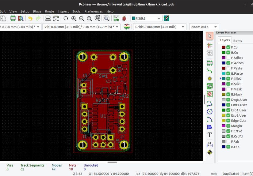
Strong tutorials lean on KiCad’s checking tools: ERC for the schematic and DRC for the PCB. Many also show how to use the 3D viewer to sanity-check part orientation, footprint scale, and mechanical collisionsbecause nothing ruins a weekend like a USB connector footprint rotated 180°.
5) Outputs: Gerbers, drills, and “yes, you really do need that file”
The finish line is manufacturing data: Gerber layers, drill files, sometimes assembly drawings, and a BOM that won’t embarrass you. Great tutorials don’t treat this as an afterthoughtthey teach you how to produce files that a fab can actually use without emailing you twenty questions.
What’s Newer on the Scene: Tutorials That Match Where KiCad Is Now
A wave of recent learning material has leaned into KiCad 9’s workflow and the expectations of modern makers: quick project setup, clearer rules, cleaner outputs, and more “do this, then check that” structure.
Distributor-grade, beginner-friendly series
Digi-Key’s KiCad 9 “getting started” content is a good example of modern pacing: it’s structured as a series that builds a real project step by step. It highlights practical layout topics like setting design rules to match manufacturing constraints, using tools like cross-probing, creating copper zones, running DRC, and checking the board in 3D. That’s the kind of detail that turns “I followed a tutorial” into “I can now ship a board.”
Fabrication-minded guides
Fabricators and PCB-focused engineering blogs increasingly publish KiCad walkthroughs that emphasize correctness: library setup, ERC/DRC discipline, and generation of production-ready outputs (Gerbers and assembly documentation). These guides tend to speak “factory,” which is useful even if you’re sending boards to a low-volume prototype house.
Creative and unconventional use-cases
Not every “KiCad tutorial” is about a conventional circuit board. Some of the most enjoyable guides show off KiCad as a design tool for PCB art, teaching techniques like importing vector art into footprints and using KiCad layers creativelyuseful skills even for standard boards because they sharpen your understanding of footprints, layers, and output control.
The Secret Weapon Most Tutorials Ignore: Add-ons, Plugins, and Quality-of-Life Tools
KiCad isn’t just “the schematic editor” and “the PCB editor” anymore. It has a growing ecosystem, including a Plugin and Content Manager that lets users discover and install add-onssuch as Python plugins, symbol/footprint libraries, and even color themesfrom repositories. If your tutorial mentions this, it’s usually a sign the author has actually used KiCad in the wild.
The practical takeaway: once you’re comfortable with core workflow, add-ons can speed up repetitive work (library handling, documentation helpers, visualization tweaks). But no plugin will save you from a bad footprint, so earn your fundamentals first.
How to Choose the Right “New KiCad Tutorial” for You
The best tutorial is the one you’ll finishand then use again with your own project. Here’s how to pick one that won’t leave you stranded halfway through a netlist.
Checklist for a tutorial worth your time
- Targets a specific major version (and says so clearly).
- Builds a real board (not just a demo screenshot that never ships).
- Includes ERC and DRC as normal steps, not optional extras.
- Shows outputs (Gerbers/drills at minimum) and explains what they’re for.
- Teaches decisions (placement strategy, rules, return paths), not only menu navigation.
Video vs. text tutorials: pick your brain’s favorite
Videos are great for seeing workflow and tool movement; text is great for precision and quick searching. Many learners do best with a hybrid: watch a video series for flow, keep a text-based repo tutorial bookmarked for exact steps and references. The “new tutorial hits the scene” type that lives in a repo is especially handy because you can skim, search, and revisit the exact step you forgot.
Common Beginner Mistakes (and How Good Tutorials Prevent Them)
The difference between a tutorial and a trap is whether it warns you about predictable mistakes. Here are the classics:
- Footprint mismatch: Your schematic symbol is correct, but your footprint has a different pin order. Better tutorials show how to detect and fix this before you route an entire board.
- Board outline confusion: New designers draw the outline on the wrong layer or forget mechanical constraints. Strong tutorials define the outline early and treat it as a real requirement.
- Design rules as an afterthought: If you set clearances after routing, you’ll be “fixing” for hours. Good guides make rules step one.
- Unrealistic placement: If your decoupling caps are social distancing from the IC, your power integrity will complain. Good guides teach placement by function.
- Skipping checks: ERC and DRC aren’t chores; they’re your personal QA department that doesn’t need coffee breaks.
Wrap-Up: A Tutorial That Teaches a Workflow Is a Gift to the Community
“A new KiCad tutorial hits the scene” isn’t just internet hype. When a tutorial is structured, version-aware, and end-to-end, it lowers the barrier to entry for everyonestudents, hobbyists, startups, and engineers crossing over from another CAD ecosystem.
If you want the fastest path to confidence, choose a tutorial that starts with a real board, forces you to run checks, and makes you generate manufacturing outputs. That’s where KiCad stops being “software you’re learning” and becomes “a tool you own.”
Extra: of Real-World KiCad Experience (So You Don’t Have to Learn the Hard Way)
The first time I followed a “full workflow” KiCad tutorial, I thought I was doing greatright up until I hit the footprints. My schematic looked pristine, like something you’d frame and hang in an electronics museum. Then I opened the PCB editor and realized half my parts were “unassigned,” a quarter were assigned to footprints that looked suspiciously like they belonged to a different universe, and one connector had pads arranged in a pattern I can only describe as “modern art.”
That’s when the best lesson clicked: KiCad isn’t one tool; it’s a chain of tools. A tutorial that’s truly helpful doesn’t let you pretend the chain doesn’t exist. It makes you create the schematic and attach footprints, then it makes you push that data into layout and reconcile the mess. It’s annoying the first timeand unbelievably empowering the second.
My biggest “aha” moment came from learning to treat design rules like guardrails, not speed bumps. Before that, I would route first, then run DRC, then stare at a terrifying list of violations like it was a breakup text. A modern tutorial that starts by setting constraints (trace widths, clearances, via sizes) changes the experience completely. Suddenly, routing feels less like guessing and more like solving a puzzle with rules that actually help you win.
I also learned to love the ratsnest. Not in a “I want it as a wallpaper” kind of way, but in a “this is a living map of my intent” way. When you place parts and the ratsnest lines shorten, you’re watching the design become physically sensible. Good tutorials teach you to place by function: keep decoupling capacitors close to power pins, keep sensitive analog sections away from noisy digital traces, and think about how current returns through ground. Even on a small board, those habits show up in whether your design is calm or chaotic.
The funniest mistake I made was silkscreen optimism. I labeled everything. Everything. Resistor values, net names, inspirational quotes, probably my grocery list. Then I zoomed out and realized my silkscreen looked like a ransom note made by a very nerdy raccoon. A good tutorial quietly teaches restraint: reference designators that are readable, polarity marks that are unmissable, and labels that help assemblynot a novella on the top layer.
And finally: the 3D viewer. I used to treat it like a vanity mirrorsomething you check only when you want to feel proud. Then I had a connector collide with a mounting hole in real life. Now I treat 3D as a sanity check, not a celebration. When a tutorial demonstrates “preview in 3D, then fix the mechanical issue,” it’s teaching you a professional habit with hobbyist tools.
The point of all this isn’t that KiCad is scary. It’s that KiCad is honest. It will let you make mistakes, but it also gives you the instruments to catch themif your tutorial teaches you to use those instruments at the right time. And once that timing becomes muscle memory, you stop needing a tutorial for every step. You start using tutorials the way pros do: as references, inspirations, and shortcuts to the next good decision.